What is Transistor
What is transistor ? Transistor is the combination of two words in meaning transfer and resistance. It consists of two back-to-back P-N junctions manufactured in a single piece of semiconductor crystal. A transistor is simply a sandwich of one type of semiconductor material between two layers of other. They are two types.
PNP Transistor
When N-type material is sandwiched between two p-type materials as shown in Fig is called PNP transistor

NPN Transistor
When p-type material is sandwiched between two N-type materials as shown in Fig NPN transistor.

The two junctions give rise to three regions called emitter labeled as E, base labeled as B, and collector labeled as C.
Emitter : (E)
It is on L.H.S. Also, it is heavily doped. Its function is to supply the majority of carriers.
Base : (B)
It is in the middle section of the transistor, it is very thin in order of 10-6m. It is very lightly doped.
Collector : (C)
It is on R.H.S. So, it collects the majority of carriers. Also, it is physically larger than it dissipates much greater power. Two junction for these three portions of transistor i.e.
- Emitter-base (E/B) Junction
- Collector–base (C/B) junction.
Transistor biasing
It must always be remembered that
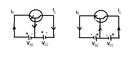
1 ) E/B junction is forward biased always
2 ) C/B junction is reverse biased always
In fig two batteries respectively provide the dc emitter supply VEE and collector supply voltage Vcc for properly biasing the two junctions.
It must be remembered that a transistor will never conduct any current if the (E/B) junction is not forward-biased.
Transistor circuit configurations
Basically, there are three types of circuit connections (called configurations) for operating a transistor.
1 ) common – base (CB)
2 ) common – emitter (CE)
3 ) common – collector (CC)
In each case, the emitter (dc) is forward-biased and the collector junction is reversed-biased. The configurations are:-
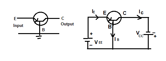
Common base configuration
In CB configuration, the base of the transistor terminal will be connected commonly between the input and the output terminals. Keeping collector base voltage(VCB) constant, variation of emitter current(IE) with base-emitter voltage(VBE),
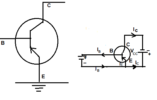
Common emitter configuration
In CE configuration, the transistor will be connected commonly with a collector terminal between the input and output terminals. Keeping collector base voltage(VCB) constant, the variation of emitter current(IB) with collector-base voltage(VCB).
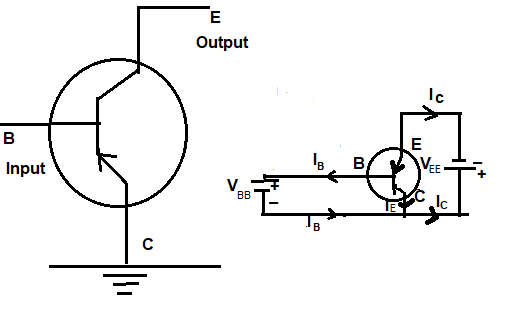
Common collector configuration
Common collector configuration
If an NPN transistor is used, the connection of the battery will be reversed to that of the PNP
Characteristics curve of a transistor
Transistor characteristics are the graphs formed by experiments that show relationships between various currents and voltages. Also, these characteristics help to see how one can use a transistor.
Input Characteristics or base characteristics
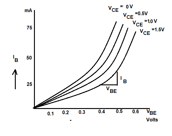
A family of the curve is obtained by plotting a graph between emitter-base voltage VBE and base current IB for the constant value of VCE. These curves show that IB is negligibly changed i.e. it is almost zero. When VBE increases ta a certain limit IB increases rapidly.
Hence, the input curve is used to determine the input transistor resistance
Rint = ΔVBE/ΔIB
Also, the input resistance for the transistor is small in the order of a few thousand ohms.
Output characteristics or collector characteristics
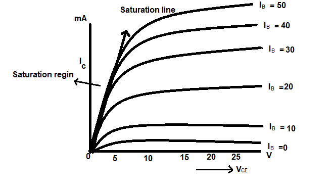
Further, the curves are obtained by plotting a graph between the emitter-collector voltage VcE and collector current Ic keeping the base current IB constant.
Hence, the curves show that the current IC increases rapidly with the increasing value of VCE. But afterward, the collector current is too slow and is almost constant. However, the collector characteristics are used to determine output resistance.
Rout = ΔVcE /ΔIc
The output resistance of the transistor is much larger than that of the input resistance.
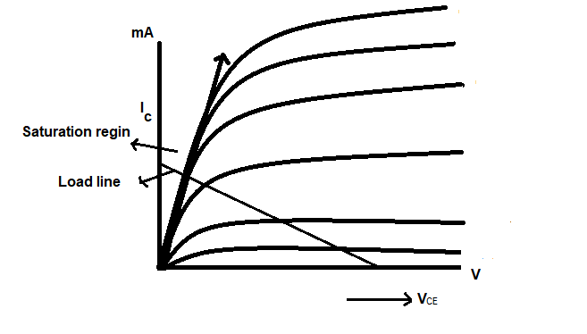
Load Line
If plot the voltage VCE on the x-axis and current IC on the y-axis, then the intercept of this line is called the load line. Also, in the saturation region, the control of the current is lost by the base.
Transistor characteristics
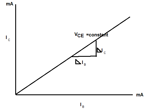
Hence, transistor characteristics is the curve obtained by plotting IC against IB keeping VBE constant. Further, this shows how IC changes with IB. So, this is described with a ratio of the change in the value of ΔIc to the corresponding change in ΔIB is called β.
i.e β=Δ Ic/ΔIB
Transistor current
Regardless of transistor type or configuration the current flowing into a transistor is taken as positive and those flowing out of it are taken as negative. So IE is positive and IB and IC are negative. Hence, by applying Kirchoff’s theorem we have
IE = IB + IC
Transistor application
There are several application
Amplification
Transistor can make signal stronger in electronic circuit, so make it suitable for further processing.
Switching
It act as electronic switch, which allow or block electric current It is based on voltages or current applied. Also, logic gate circuit a based on this switching.
Signal Modulation
It can modulate signals. As in FM (frequency modulation) used in radio transmitters.
Voltage Regulation
It is used in electronic as voltage regulator, which result stable output voltage.
Transistor played a vital role in electronic circuit which is now more in compact form than pervious periods. So, it has fundamental component and role in current electronic world. Also, its development is continuously over the years.
Further read next topic about Diode
Further read next topic about Electronic
