Electronic city
The study, design, and use of devices that depend on the conduction of electricity through a vacuum, gas, or semiconductor material are called the definition of electronics.
What are conductors
The solid materials which conduct electric current easily are called conductors. Conductors have plenty of free electrons and are easily available for electric conduction. Examples of good conductors are gold, silver, copper, aluminum, etc. These substances have a resistivity of the order of 10-4 Ω-m.
What are insulators
The solid materials which do not conduct electric current at all are called insulators. These materials have a few electrons available for the conduction of electric current. Examples of insulators are mica, rubber, glass, etc. The value of resistivity for insulators is of the order of 108 Ω- m.
What are semiconductors
A semiconductor is a material that is either a good conductor or a good insulator. These materials are b/w conductors and insulators. Semiconductor materials examples are germanium and silicon. The resistivity of semiconductor material is of the order of 10+4 Ω- m.
Explanation of conductors, semiconductors, and Insulators in terms of energy bands
Insulators
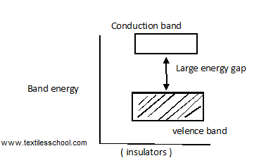
The electrical conduction properties of different elements can be studied in terms of electrons having energies in the valance and conduction bands. The electrons lying in lower energy bands, which are normally filled, play no part in the conduction process. In insulators, valence electrons are bound very tightly to the parent atoms they require a very large electric field to remove them from the attraction of their nuclei, which means insulation has,
- Full valance band
- An empty conduction band
- A large energy gap b/w two bands.
For conduction to take place electron must give sufficient energy to jump from the valence band to the conduction band so the ordinary electron can not jump from the lower to the upper band in insulators.
Conductors
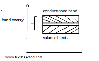
In conductors, the valence and conduction bands overlap each other as shown in Fig. In fact, there is no physical distinction b/w the band. Items a large no of conduction electrons available. The important point is the absence of an energy gap there is no structure for establishing the holes. The total current flow is the flow of electrons only. The fig shows the energy bands in conductors overlapping
Semiconductors
In semiconductor materials at room temperature, there are
- Partially filled conduction band.
- Partially filled valance band.
- Between two band a very energy gap.
At absolute temperature, the valence band is completely filled and the conduction band is completely empty so the semiconductor material acts as an insulator. With an increase in temperature, the two bands come close to each other. The gap between the two bands come small or moderate at room temperature. So if a small amount of energy is given the conduction comes much more.
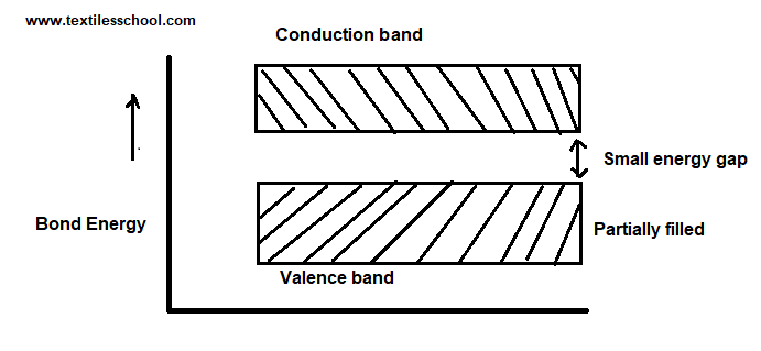
The energy gap is about 1 e.v in semiconductors.
Types of semiconductors
- Semiconductors
- Intrinsic /pure semiconductors
- Extrinsic/impure semiconductors
- N-Type
- P-Type
Intrinsic semiconductors
An intrinsic semiconductor is one that is made of semiconductor material in an extremely pure form. A common example of intrinsic semiconductors is pure germanium and silicon.
Structures of germanium or silicon
In a Germanium crystal, each atom has four electrons in the outermost shell. Ge belongs to group iv. It shares four electrons with other atoms making covalent bonds. So its configuration is stable and there is no free electron available and the conduction band is empty. However the
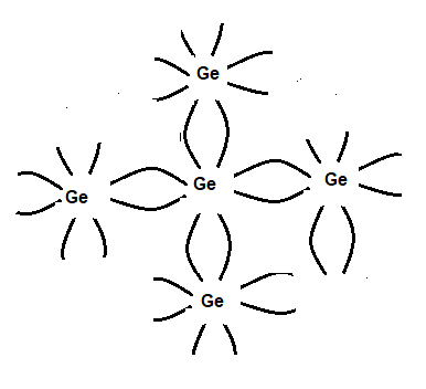
The forbidden energy gap is very narrow only 101 e.v (electron volt). In the case of silicon only 0.72 e.v. The energy gap is so small that even at room temperature they possess a sufficient amount of energy gap from the valence to the conduction band. However, when an electron is liberated into the conduction band a hole is created in the valence band. The hole is positively charged. Now when an electric field is applied across the intrinsic semiconductor at a temperature greater than ok conduction electrons move to the anode and the holes in the valence band move to the cathode. Thus semiconductor current consists of The movement of electrons and holes in opposite directions in the conduction and valence bands respectively, or, the intrinsic semiconductor may be defined as one in which the number of holes is equal to the number of conduction electrons.
An intrinsic semiconductor at room temperature
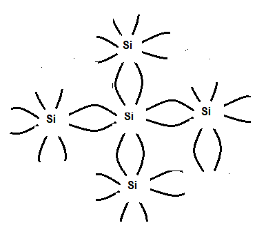
Thus germanium and silicon are examples of (pause) intrinsic semiconductors
What are holes
The hole represents the absence of a negative charge and is attractive to electrons. It has a positive charge equal to a negative charge electron in magnitude.
Extrinsic semiconductors
These intrinsic semiconductors to which some suitable impurity or doping agent has been added in an extremely small amount ( about 105~108 ) are called extrinsic or impure semiconductors.
What is doping?
The addition of impurity to an intrinsic semiconductor, this process is called doping.
What are donor atoms?
What are donor impurities?
The pentavalent atoms like ( Bi, Sb, As, P, etc.) lose or donate their fifth extra electron to the conduction band of pure germanium. Their pentavalent doping atom is known as the donor atom. These are considered donor impurities
What are acceptor Impurities?
Trivalent atoms like ( Ga, In, Al, B, etc. ) accept one electron from the germanium atom. Thus there are called acceptor impurities.
The fact that why doping materials are called impurities is that they alter the structure of pure semiconductor materials.
N-type semiconductors
An N-type semiconductor is obtained by adding an impurity like antimony (Sb) to a pure germanium structure. As shown in Fig. each atom of antimony forms covalent bonds with the surrounding four atoms of germanium with the help of four of its five electrons. The fifth electron is loosely bound to the antimony atom and is relatively free. Hence it can be excited from the valence to the conduction band giving a small amount of isothermal energy or electric field.
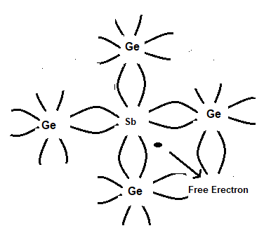
The addition of antimony to pure germanium makes it an N-type semiconductor. In giving an electron antimony atom becomes positively charged or a hole is produced, but it could not take part in the conduction because it is firmly tied to a crystal lattice. The addition of antimony increases the free electrons and conduction electrons are increased.
Thus in an N-type semiconductor current flows due to an excess of free electrons. The amount of impurity to be added is about 1 atom in 107 atoms of germanium.
It may also be seen in N-type semiconductors electrons are the majority of carriers and holes as minority carriers.
P-type semiconductors
A P-type semiconductor is obtained by the addition of traces of a trivalent impurity like boron (B). In this case, the three valence electrons of the boron atom form covalent bonds with four surrounding germanium atoms but one bond is left behind or incomplete and it creat a hole as shown below.
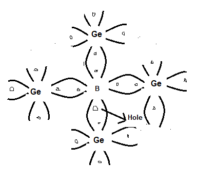
Thus the addition of boron to pure germanium makes it a positively charged or P-type semiconductor. The addition of boron causes as many holes as there are boron atoms. The concentrations of holes are greater now than that of electrons in the conduction bond. Thus the current flow in P-type semiconductors is due to holes which are also the majority carriers and electrons are the minority carriers.
What is the P-N junction?
What is a semiconductor diode?
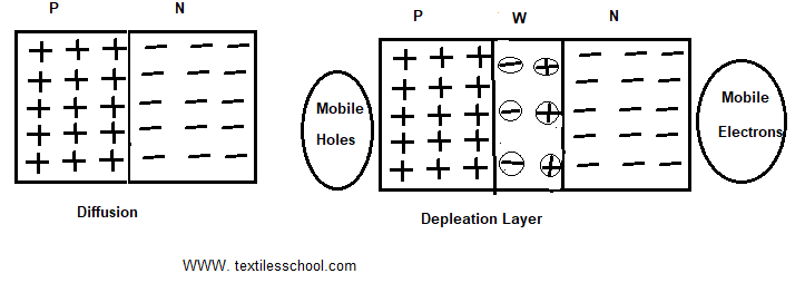
When a single piece of a semiconductor like Ge or Si is doped one half by P-type impurities and another half by N-type impurities as shown in fig.
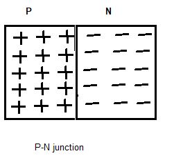
The plan dividing the two halves or zones is called the P-N junction takes place.
- formation of the depletion layer
- junction barrier
potential VB is developed. A P-N junction or semiconductor diode has the ability to allow current to flow only in one direction. The flow of current in the opposite direction is practically zero.
Formation of the depletion layer
When a P-N junction is formed. In the p-region and electrons are minority carriers, holes are majority carriers; in the N-region, electrons are majority carriers and holes are minority carriers. Since this difference in concentration establishes a density gradient across the junction resulting diffusion of majority carriers. Holes diffuse from the P to the N region and electrons diffuse from N to the P region. So, this recombination of free and mobile holes and electrons produces the marrow region at the junction called the depletion layer. It has a width of about /um or 10-3mm or 10-6m. The depletion layer has only fixed and immobile ions as shown in Fig.
Junction/barrier voltage
It is denoted by VB. Also, it is due to the charge separation. So, it is established even junction terminals are not connected to any external source of e.m.f. So, its value at room temp for Ge is 0.3V and
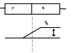
for Si 0.7 V respectively. Its value depends on doping density, electronic charge, and temperature. As long as harrier voltage exists, there is no flow of charge in the P-N junction.
Effect of temperature on Barrier voltage(VB)
Barrier voltage has a temperature decrease at a rate of 2 mV/C0. Also, silicon junction can operate up to 100oc and Ge at 75oC.
Forward-biased P-N Junction
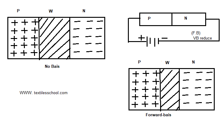
When the positive terminal is connected to the P region and the negative terminal is connected to the N region as shown in Fig, the junction is said to be forward-biased. Also, it permits an easy flow of current across the junction. The current flow in the forward direction is greater due to this reason.
As soon as the battery connection is made ( applied external voltage ) the barrier potential is reduced which now allows more current to flow across the junction. Since in forward biased junction the thickness of the depletion layer is reduced.
Reverse-biased P-N junction
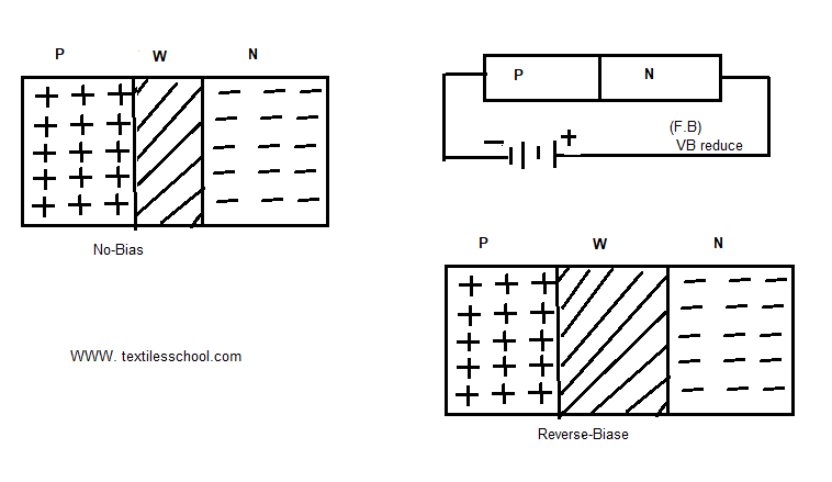
When the positive terminal is connected to the negative region and the negative terminal is connected to the P-region as shown in Fig. Also, the function is said to be reverse-biased. In this case, the potential barrier is increased due to applied voltage, therefor it offers high resistance because the depletion layer is increased.
What is the P-N Junction breakdown?
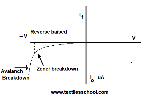
If the revered bias of a PN junction has increased a point will be reached when the junction breaks down and the reverse current sharply rises to a value only by the external resistance in series with the junction. Hence, this critical value of junction voltage is called the breakdown voltage.
The following are two mechanics responsible for a breakdown under increasing reverse voltage.
Zener breakdown
It takes place in that junction which is heaving doped and has a narrow depletion layer. So, the breakdown voltage sets a strong electric field of 108V/m across the layer which is responsible for rupturing covalent bonds and generating electron-hole pairs. Even a small further increase in reverse voltage is capable of producing current carriers. That is why Zener breakdown has a low value of resistance in the junction.
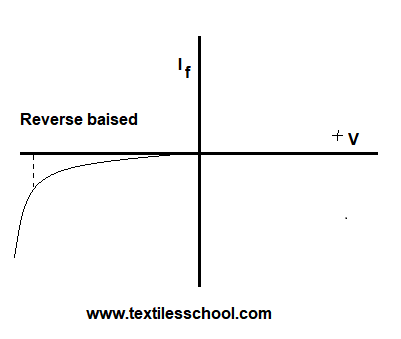
Avalanch breakdown
It takes place in lightly doped having wide depletion regions, so the electric field is not allowed to create Zener breakdown under the electric field minority carriers strike with covalent bonding depletion region, and electron hole-pair are generated so these generated holes and electrons collide with covalent bonds in the depletion region and more current flow. Since the two breakdown phenomena are shown in Fig.
Characteristics curve of a diode
Characteristics curve of a P-N junction
The forward and reverse voltage current. Characteristics are shown in Fig. Thus characteristic curve is simply a plot of current as a function of plate potential.
Furthermore, the flow of current in the forward direction is in excess and current flows easily in the forward junction. It is found that a very small current ( a few micrometers) flows even when the junction is reverse-biased.
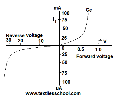
It can be seen in the beginning there is a slight increase in reverse current with an increase in reverse voltage. If the reverse bias is increased beyond a critical value there is a sudden increase in reverse current due to the breakdown of the crystal structure. This reverse voltage is also known as a breakdown.
Further read next topic about Transistor
Also, Further read next topic about Diode
Further read next topic about Application of diode
