Diode dynamics
A diode is divided into the following types
- Zener diode
- Tunnel diode
- Varactor
- PIN diode
- Schottky diode
- Step recovery diode
- Thermistors
- L.E.D ( Light Emitting diodes)
- Avalanche photodiode
Zener diode
Zener diode is reverse biased, heavily doped. It can be used as voltage regulation a peak clipper, and power protection of meters in different circuits. ( schematic symbols of Zener diode )
Tunnel diode
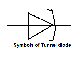
It is one thousand times heavily doped P-N junction. Its depletion layer is 0.00001 mm. Its breakdown voltage is 0.5 V, the thin depletion layer reduces the breakdown voltage. Further, it can be made by Ga-As or Ga-Sb. Also, it is used to alter high switching in order of 10-9, micro meter oscillators, and low noise circuits. So, it is easy to operate, at high speed and is also insensitive to nuclear radiation
( symbol of tunnel diode )
Varactor
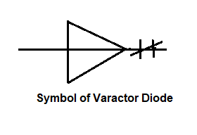
It is a voltage-dependent variable capacitor. Also, it is alternatively known as varicap. So, it is also known as a voltage variable capacitor diode i.e (vvc) It is used for automatic frequency control, as an F.M. modulator, adjustable band-pass filter, and as a parametric amplifier.
( symbol of v.v.c )
PIN diode
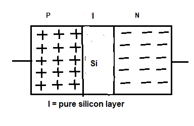
Pin diode is made by a P-N junction but sandwiched between them is an intrinsic layer of pure silicon. Also, it can be used as a faster response capable of generating very weak signals. So, pin diode can be used at more than 300 MHZ frequency.
( I = pure silicon layer )
Schottky diode
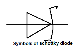
Schottky diode is also called the Schottky barrier and hot barrier. It is a unipolar, electrons are the majority carriers. Where electrons move in both directions. Schottky diode is a fast switcher.
( symbol of Schottky diode )
Step recovery diode
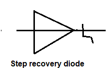
Step recovery diode is used for a strong electric field on both sides, a high-frequency harmonic generator, and very fast pulsing. Its symbol is
Thermistors
Thermistor is a temperature-dependent resistor. (explained in a resistor )
L.E.D ( Light Emitting diodes)
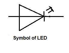
LED diode is forward biased P-N junction. Which emits light when it is energized. LED diode is made up of Ga-P, Ga-As, P, and Ga-As. Ga-P has the red or green light. Ga-As has invisible radiation ( amber ) light. These are used in digital watches, calculators, and alarm systems. Its works at 1.5 to 3.3 v.
(symbol of L.E.D)
Avalanche photodiode
Avalanche photodiode operates at the avalanche breakdown region. It is ultrafast and can be used at a frequency of a few GHz with an excellent signal of input noise ratio.
Diode as a rectifier
Rectification
Converting AC voltage into DC voltage is called rectification, alternating current into the pulsating current.
Half-wave rectifier
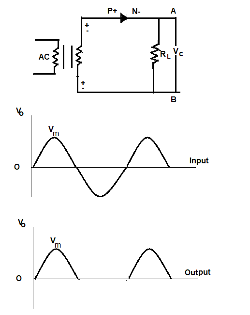
As shown in figure the basic half wave rectifier diode circuit. a single diode is used with RL. During the positive half cycle of the input ac voltage, it is forward-biased and current flows through it i.e. it conducts, hence positive half cycle gives output voltage Vo as shown in fig.
During the negative half, there is no current flow because no diode is reversed-biased. Hence there is no voltage drop Vo across RL i.e vo = 0.
The negative input half cycle is suppressed i.e. it is not utilized for delivering power to load. Since only, one-half cycle of the input wave is used, it is called a half-wave rectifier ( Transformer is only optional ).
Full-wave rectifier
In this case, both half-cycles of input are utilized with the help of two diodes working alternately. For full-wave rectification transformer is essential.
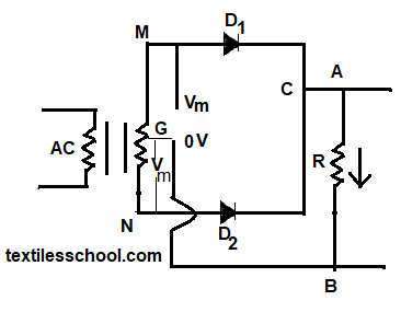
The full wave rectification circuit with a center-tapped transformer is shown in Fig.
The center tapped is usually taken as the ground or zero voltage reference point. When the input switch is on, the ends M and N become positive and negative alternately. During the positive half-cycle of the ac-voltage terminal, M is +ve G at zero potential. Hence being forward biased D1 conducts but not D2 which is reversed biased. So cannot flow along MD1, CABG. As a result, the positive half cycle of the voltage aped appears across RL.
In the negative half cycle, when terminal N becomes +ve D2 conducts but no D1, and current flows along ND2CABG. So current flows through RL in the same direction from A to B in both half cycles of ac input. Hence, it means both half cycles of input ac supply are utilized, this is called full-wave rectification.
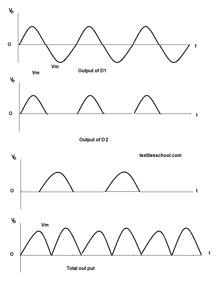
Also, in half-wave rectification, only a pulsating dc wave having a ripple frequency equal to that of the input voltage frequency is obtained. But in full-wave rectification, the frequency of the rectified output voltage is twice the supply frequency.
The following up curves explain the input and output voltage of the full wave rectifier.
Further read next topic about Transistor
Also, Further read next topic about Electronic
Further read next topic about Application of diode

