What is the application of a diode?
Application of diode has an unlimited range, due to its ability to control the circuit voltage and current. The diode can flow current in one direction and block in reverse. Below are just some examples of the application of diode. In electric engineering, different types of diodes are designed for a wide range of applications.
Application of diode
- It can be used as a rectifier. it converts AC to DC.
- It is used for the modulation and demodulation of small signals in communication circuits.
- It is used as a voltage-stabilizing circuit. Zener diode is used for this purpose.
- It can be used as a capacitance change with reverse biased voltage in a varactor diode.
- A diode is used to limit the amplitude of AC signals. This can often used in audio and video signal distortion. And also protects from overvoltage.
- A diode is used as protection in the circuit from overcurrent or voltage, which protects from sensitive circuit from breaking.
- In radio and microwave frequency mixing and frequency conversion diode is used.
- LED is a special type of diode that emits light when the current flows in them. LED circuit is used in various application like indicator, lights, display, and optic data.
- A diode is used for photodetection, which is exposed to light to generate current. A photodetection diode is used in light sensors and optical instruments.
- Schottky diode is used in high-frequency light speed switching.
- Diode used as surge current or voltage as a protection for sensitive circuits.
- The diode is used for voltage clipping. It can limit voltage to a certain level, not exceeding the threshold.
- It is used to make certain logic gates as OR, AND, and NOT gates.
- It is used as a high voltage multiplier, which is used in digital circuits, an example are Cockcroft-Walton multiplier.
- A diode is used in temperature measurement, voltage drops when temperature rises.
Fabrication of diode
The following diode fabrication methods may be used to produce a P-N junction.
- Grown junction
- Alloy junction
- Defused junction
- Epitaxial growth
- Point contact junction
Grown Junction
Since such junctions are prepared diode fabrication by applying the Czochralski or floating zone technique. Also, the apparatus used for the Czochralski technique is shown in Fig.
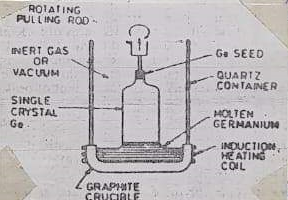
Further, molten semiconductor material in a cubical form is dipped as a single crystal seed of the desired impurity level. Then it is gradually withdrawn while the shaft holding the seed is slowly turning. When the crystal is pulled out, impurities of P-and N-type are alternately added. To produce a P-N junction, this large area crystal is then cut into a large number of smaller area diodes.
Alloy junction
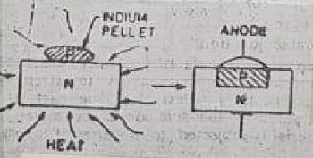
Firstly, the junction produced in this process has large junction capacitance and current ratings. Furthermore, in this process, a ting dot of indium is placed on the surface of N-type silicon and the two are heated well above the melting point of Indium. Further, the two metals are in a molten state, and Induce dissolves some of the silicon. The temp. is then lowered. P-N junction crystal is formed as shown in Fig.
Diffused junction
Furthermore, the diffusion process is of two types
Solid diffusion
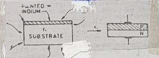
The solid diffusion process starts with the painting of a P-type impurity on an N-type substrate and heating the two until the impurity diffuses to a sheet distance into the substrate to form a P-type layer.
Gaseous diffusion
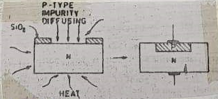
In this process, N-type material is heated in a chamber containing a high concentration of an acceptor impurity in vapor form some of the acceptor atoms are diffused into the N-type substance to form a P-type layer thus a P-N type junction is formed. Also, the size of the P-region can be controlled. So, the figure shows the complete process.
Epitaxial junction
Firstly, this junction has low resistance. Moreover, the junctions are grown on top of an N-type wafer in a temperature chamber. The growth proceeds atom by atom and hence a crystal lattice of junction like that of the wafer.
Point contact junction
It consists of an N-type Ge or Si wafer about 1.25mm square by 0.5mm thick, one face of which is soldered to a metal base by radio frequency by heating as shown in Fig.
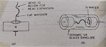
Also, the other face has a tungsten spring or phosphor bronze pressed against it is called a cat’s whisker. The P-N junction is formed by passing a large current for one or two seconds through the wire, Thus p-type material is shown in Fig (a). Also, the capacitance junction is very low
Further, read the next topic about Transistor
Also, Further read the next topic about Diode
Further, read the next topic about Electronic